The issues facing the semiconductor industry as they relate to interconnects are profoundly impacted by the ever-shrinking dimensions of regular process technology. The standard interconnect material, copper, has been used for the past 30 years and is now reaching commercial end-of-life due to Moore’s Law and electron migration that renders copper extremely problematic in low geometry fabrication. At sub-15 nm interconnect dimensions, the resistivity of copper increases rapidly – causing significant degradation in both circuit and system-level performance, power, and dramatically impacting all reliability metrics required by modern semiconductor designs in products such as GPUs, CPUs and others.
The startup chose to use graphene as a basis for their technology. While tiny flakes of graphene are easy to produce, attempts to scale the manufacturing process for integration into mainstream CMOS have had negligible success due to fab-compatibility issues and quality control concerns. Large area graphene synthesis, typically involving chemical vapor deposition (CVD) based techniques, requires high temperatures that far exceed the allowed thermal budget of CMOS interconnect fabrication, and also require a mechanical “transfer” of the graphene grown over a metallic substrate to dielectric substrates.
Moreover, pristine (monolayer) graphene is a semimetal with a low charge carrier density, resulting in high sheet resistance, which further limits its direct applicability to interconnect applications. Therefore, for interconnect applications, multiple layers of edge-contacted graphene along with suitable “intercalation-doping” is required.
This was first theorized and experimentally demonstrated by Destination 2D’s CTO and his team, who subsequently pioneered the pressure-assisted solid-phase diffusion technique for synthesizing multilayered graphene directly over dielectric substrates at CMOS-compatible temperatures.
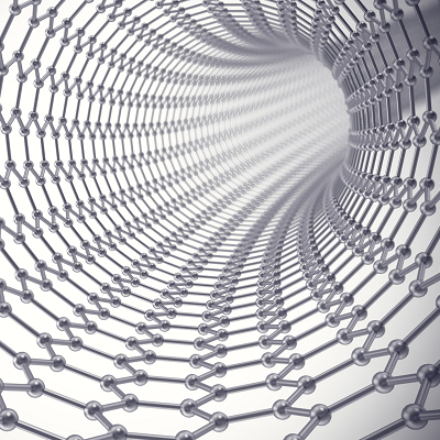
Destination 2D’s CMOS-compatible interconnect design innovation is achieved via intercalation-doped and edge-contacted multi-layer graphene, which delivers lower resistivity, significantly better reliability and up to 80% higher energy-efficiency than copper interconnects.
A CMOS-compatible synthesis technology allows for the direct synthesis of graphene onto wafer-scale dielectric substrates at temperatures significantly below the CMOS thermal budget. All of this is achieved without the warping and cracking issues that have plagued previous graphene commercialization efforts around CMOS interconnects.
Armed with several key patents, these design and process technology inventions are just one aspect of Destination 2D’s breakthrough innovation. The other equally crucial component is the CoolC GT300, a specialized, industrial-scale patented equipment developed by Destination 2D.
The CoolC GT300 implements Destination 2D’s proprietary graphene synthesis process without the traditional thermal issues that have prevented graphene from being in CMOS applications. Simultaneous with Destination 2D’s achievement of the wafer-scale graphene synthesis technology, this patented equipment is announced with immediate availability for order to interested customers.
“Wafer-scale graphene coverage demonstrated by Destination 2D using BEOL compatible low-temperature transfer-free process marks a significant milestone for the CMOS industry,” said Ravi Iyengar, CEO of Destination 2D. “Destination 2D’s interconnect technology – when integrated in both Logic and Memory chips – could profoundly transform the landscape for Artificial Intelligence and other compute-centric applications.”
Read the original article on Graphene-Info.


