These properties have made graphene increasingly important in applications across various fields, including electronics, energy storage, medical technology, and, most recently, quantum computing.
Graphene’s quantum properties, such as superconductivity and other unique quantum behaviors, are known to arise when graphene atomic layers are stacked and twisted with precision to produce “ABC stacking domains.” Historically, achieving ABC stacking domains required exfoliating graphene and manually twisting and aligning layers with exact orientations—a highly intricate process that is difficult to scale for industrial applications.
Now, researchers at NYU Tandon School of Engineering led by Elisa Riedo, Herman F. Mark Professor in Chemical and Biomolecular Engineering, have uncovered a new phenomenon in graphene research, observing growth-induced self-organized ABA and ABC stacking domains that could kick-start the development of advanced quantum technologies. The findings, published in a recent study in the Proceedings of the National Academy Of Sciences (PNAS), demonstrate how specific stacking arrangements in three-layer epitaxial graphene systems emerge naturally — eliminating the need for complex, non-scalable techniques traditionally used in graphene twisting fabrication.
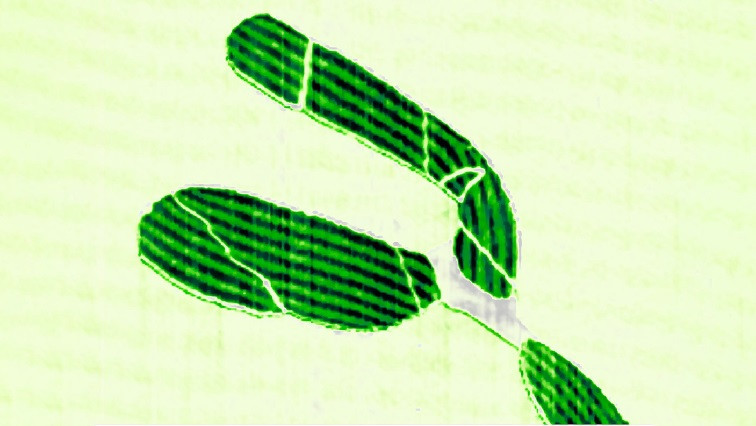
These researchers, including Martin Rejhon, previously a post-doctoral fellow at NYU, have now observed the self-assembly of ABA and ABC domains within a three-layer epitaxial graphene system grown on silicon carbide (SiC). Using advanced conductive atomic force microscopy (AFM), the team found that these domains form naturally without the need for manual twisting or alignment. This spontaneous organization represents a significant step forward in graphene stacking domains fabrication.
The size and shape of these stacking domains are influenced by the interplay of strain and the geometry of the three-layer graphene regions. Some domains form as stripe-like structures, tens of nanometers wide and extending over microns, offering promising potential for future applications.
“In the future we could control the size and location of these stacking patterns through pregrowth patterning of the SiC substrate,” Riedo said.
These self-assembled ABA/ABC stacking domains could lead to transformative applications in quantum devices. Their stripe-shaped configurations, for example, are well-suited for enabling unconventional quantum Hall effects, superconductivity, and charge density waves. Such breakthroughs pave the way for scalable electronic devices leveraging graphene's quantum properties.
This discovery marks a major leap in graphene research, bringing scientists closer to realizing the full potential of this remarkable material in next-generation electronics and quantum technologies.
Read the original article on NYU Tandon School of Engineering.

