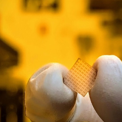
This enhanced efficiency UVC microLED has showcased the viability of a lowered cost maskless photolithography through the provision of adequate light output power density, enabling exposure of photoresist films in a shorter time.
Conducted under the supervision of Prof. KWOK Hoi-Sing, Founding Director of the State Key Laboratory of Advanced Displays and Optoelectronics Technologies at HKUST, the study was a collaborative effort with the Southern University of Science and Technology, and the Suzhou Institute of Nanotechnology of the Chinese Academy of Sciences.
A lithography machine is crucial equipment for semiconductor manufacturing, applying short-wavelength ultraviolet light to make integrated circuit chips with various layouts. However, traditional mercury lamps and deep ultraviolet LED light sources have shortcomings such as large device size, low resolution, high energy consumption, low light efficiency, and insufficient optical power density.
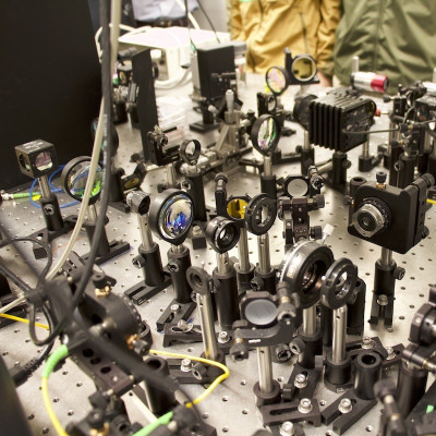
To overcome these challenges, the research team built a maskless lithography prototype platform and used it to fabricate the first microLED device by using deep UV microLED with maskless exposure, improving optical extraction efficiency, heat distribution performance, and epitaxial stress relief during the production process.
Prof. Kwok highlighted, “The team achieved key breakthroughs for the first microLED device including high power, high light efficiency, high-resolution pattern display, improved screen performance and fast exposure ability. This deep-UV microLED display chip integrates the ultraviolet light source with the pattern on the mask. It provides sufficient irradiation dose for photoresist exposure in a short time, creating a new path for semiconductor manufacturing.”
“In recent years, the low-cost and high-precision maskless lithography technology of traditional lithography machines has become an R&D hotspot because of its ability to adjust the exposure pattern, provide more diverse customization options, and save the cost of preparing lithography masks. Photoresist-sensitive short-wavelength microLED technology is therefore critical to the independent development of semiconductor equipment,” Prof. Kwok explained.
“Compared with other representative works, our innovation features smaller device size, lower driving voltage, higher external quantum efficiency, higher optical power density, larger array size, and higher display resolution. These key performance enhancements make the study a global leader in all metrics,” Dr. FENG Feng, postdoctoral research fellow at HKUST’s Department of Electronic and Computer Engineering (ECE), concluded.
Their paper, titled “High-Power AlGaN Deep-Ultraviolet Micro-Light-Emitting Diode Displays for Maskless Photolithography”, has been published in the top journal Nature Photonics. It has since earned wide recognition in the industry and was named by the 10th International Forum on Wide Bandgap Semiconductors (IFWS) as one of the top ten advances in China’s third-generation semiconductor technology in 2024.
Looking forward, the team plans to continue enhancing the performance of AlGaN deep ultraviolet microLEDs, improve the prototype, and develop 2k to 8k high-resolution deep ultraviolet microLED display screens.
Read the original article on Hong Kong University of Science and Technology (HKUST).


